| ftp.delorie.com/pcb/bus-pins.html | search |
This is an idea from a while back...
Currently, gschem's symbols have single-net pins. Why not pins that reflect multiple signals? I call these "bus pins".
        +---------
        |
     ===| D[15:0]
        |
     ---| CS
        |
        +---------
The idea is that the "bus" graphic becomes a way of actually grouping signals. The trouble, of course, is algorithmically determining the connectivity. One way that might work is if the bus has an attribute (like net's "netname") that tells the group of signals, either a comma-separated list, or a numeric range (like the example above). The example above, the bus contains nets D15, D14, D13, ... D0 - in that order. So, connecting a D[15:0] pin to a D[0:15] bus does a bit-endian-swap. We'll need a bit-reversal thing for busses:
            _____
        ___|__ __|___
D[15:0] ___|__X__|___ D[0:15]
           |_____|
Alternately, gnetlist could be smart enough to see that you're pulling out D[0:15] and just pull out the signals in the right order.
 D[15:0] ======**==== D[15:0]
               ||
               \\==== D[0:15]
The tricky part is allowing for mis-matched net names, like hooking a ram chip's D[7:0] to a cpu's D[15:8] when you pair up ram chips to make wider busses. I think gnetlist needs to look at the list of signals in order, and combine them that way.
The other thing that would be nice is if three-way junctions of busses allowed for different-sized busses on each branch, such as pulling out D[7:0] from a D[15:0] bus. gnetlist will need to be smart enough to look at each branch and see what "make sense". Mapping signals in a bus to signals on a bus pin will always have to have the right number of signals, though - you can't have a D[7:0] bus attach to a D[15:0] pin; that's an error.
So, if you have an MCU with a bus pin named DBUS[15:0] and you attach a bus to it and name the bus D[15:0], you can then branch that bus to two ram chips, name one bus branch D[7:0] and the other D[15:8], and connect those branches to two ram chips with bus pins named DB[7:0]. Meanwhile, you have a bus pin A[23:0] on the CPU where you branch out A[23:16] to chip select logic, A[15:1] goes to each ram chip's A[14:0], and A0 goes to the ram bank select logic.
Pulling a net from a bus should work the same way it currently does, because the net will need to be named anyway to indicate which signal is being pulled out. I suppose a check could be added to make sure the signal being pulled out exists in the bus.
We'll need a way to branch a bus without creating the third branch; perhaps an unnamed stub branch that isn't connected? I think that's a reasonable visual representation of branching a sub-bus from a main bus.
 D[15:0] ======**==== (unnamed)
               ||
               \\==== D[7:0]
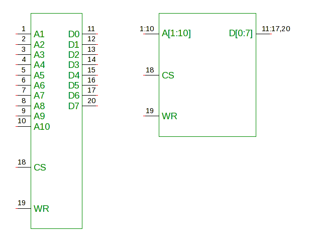
As for pin numbering at the symbol, the pin number would have the same type of grouping syntax that the bus names have, so you can map multiple physical pins to one symbolic pin:
| webmaster | delorie software privacy |
| Copyright © 2010 | Updated Aug 2010 |